 | ÐлекÑÑоннÑй компоненÑ: LTC3731 | СкаÑаÑÑ:  PDF PDF  ZIP ZIP |
Äîêóìåíòàöèÿ è îïèñàíèÿ www.docs.chipfind.ru
1
LTC3731
3731fa
APPLICATIO S
U
TYPICAL APPLICATIO
U
FEATURES
DESCRIPTIO
U
, LTC and LT are registered trademarks of Linear Technology Corporation.
Burst Mode, OPTI-LOOP and PolyPhase are registered trademarks of Linear Technology
Corporation. Stage Shedding is a trademark of Linear Technology Corporation.
*Protected by U.S. Patents including 5481178, 5929620, 6177787, 6144194, 6100678,
5408150, 6580258, 6462525, 6304066, 5705919.
The LTC
®
3731 is a PolyPhase
®
synchronous step-down
switching regulator controller that drives all N-channel ex-
ternal power MOSFET stages in a phase-lockable fixed fre-
quency architecture. The 3-phase controller drives its
output stages with 120° phase separation at frequencies of
up to 600kHz per phase to minimize the RMS current losses
in both the input and output filter capacitors. The 3-phase
technique effectively triples the fundamental frequency,
improving transient response while operating each control-
ler at an optimal frequency for efficiency and ease of ther-
mal design. Light load efficiency is optimized by using a
choice of output Stage Shedding or Burst Mode operation.
A differential amplifier provides true remote sensing of both
the high and low side of the output voltage at the point of
load. The precision reference supports output voltages from
0.6V to 6V.
Soft-start and a defeatable, timed short-circuit shutdown
protect the MOSFETs and the load. Current foldback
provides protection for the external MOSFETs under
short-circuit or overload conditions.
3-Phase Current Mode Controller with Onboard
MOSFET Drivers
±5% Output Current Matching Optimizes Thermal
Performance and Size of Inductors and MOSFETs
Differential Amplifier Accurately Senses V
OUT
±1% V
REF
Accuracy Over Temperature
Reduced Power Supply Induced Noise
±10% Power Good Output Indicator
250kHz to 600kHz Per Phase, PLL, Fixed Frequency
PWM, Stage Shedding
TM
or Burst Mode
®
Operation
OPTI-LOOP
®
Compensation Minimizes C
OUT
Adjustable Soft-Start Current Ramping
Short-Circuit Shutdown Timer with Defeat Option
Overvoltage Soft Latch
Adjustable Undervoltage Lockout Threshold
Selectable Phase Output for Up to 12-Phase Operation
Available in 5mm × 5mm QFN and 36-Pin Narrow
(0.209") SSOP Packages
Desktop Computers and Servers
High Performance Notebook Computers
High Output Current DC/DC Power Supplies
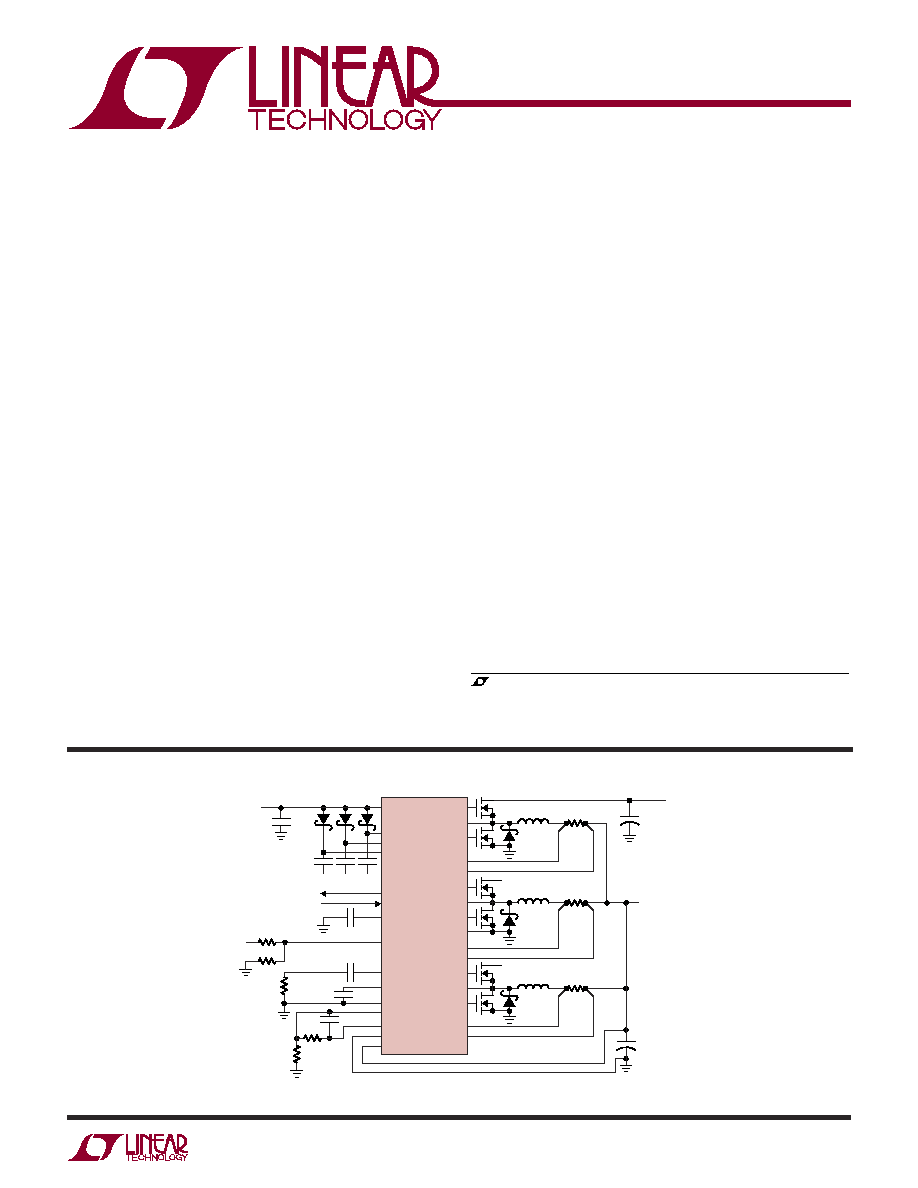
Figure 1. High Current Triple Phase Step-Down Converter
V
IN
0.003
0.8µH
22µF
35V
0.003
0.8µH
V
IN
0.003
C
OUT
470µF
4V
V
OUT
1.35V
55A
V
IN
5V TO 28V
0.8µH
V
IN
3731 F01
TG1
V
CC
0.1µF
SW3 SW2 SW1
SW1
BG1
SENSE1
+
SENSE1
BOOST1
BOOST2
BOOST3
TG2
SW2
BG2
PGOOD
PLLIN
PLLFLTR
I
TH
0.01µF
680pF
5k
OPTIONAL SYNC IN
POWER GOOD INDICATOR
RUN/SS
SGND
EAIN
DIFFOUT
PGND
UVADJ
SENSE2
+
SENSE2
TG3
SW3
BG3
SENSE3
+
SENSE3
IN
IN
+
+
10µF
V
CC
4.5V TO 7V
+
LTC3731
36k
12k
7.5k
100pF
6.04k
3-Phase, 600kHz,
Synchronous Buck Switching
Regulator Controller
2
LTC3731
3731fa
ABSOLUTE AXI U RATI GS
W
W
W
U
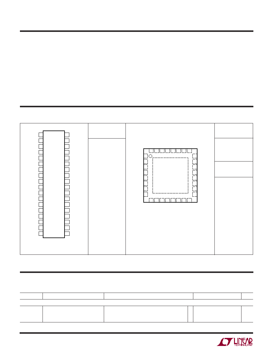
PACKAGE/ORDER I FOR ATIO
U
U
W
ELECTRICAL CHARACTERISTICS
Topside Driver Voltages (BOOST
N
) ............ 38V to 0.3V
Switch Voltage (SW
N
)................................... 32V to 5V
Boosted Driver Voltage (BOOST
N
SW
N
) .... 7V to 0.3V
Peak Output Current <1ms (TG
N
, BG
N
) ..................... 5A
Supply Voltages (V
CC
, V
DR
), PGOOD
Pin Voltage .................................................. 7V to 0.3V
RUN/SS, PLLFLTR, PLLIN, UVADJ,
FCB Voltages ............................................. V
CC
to 0.3V
ORDER PART
NUMBER
LTC3731CG
LTC3731IG
1
2
3
4
5
6
7
8
9
10
11
12
13
14
15
16
17
18
TOP VIEW
G PACKAGE
36-LEAD PLASTIC SSOP
36
35
34
33
32
31
30
29
28
27
26
25
24
23
22
21
20
19
V
CC
PLLIN
PLLFLTR
FCB
IN
+
IN
DIFFOUT
EAIN
SGND
SENSE1
+
SENSE1
SENSE2
+
SENSE2
SENSE3
SENSE3
+
RUN/SS
I
TH
UVADJ
CLKOUT
PGOOD
BOOST1
TG1
SW1
BOOST2
TG2
SW2
V
DR
BG1
PGND
BG2
BG3
SW3
TG3
BOOST3
PHASMD
SGND2
T
JMAX
= 125°C,
JA
= 95°C/W,
JC
= 32°C/W
Consult LTC Marketing for parts specified with wider operating temperature ranges.
The
denotes the specifications which apply over the full operating
temperature range, otherwise specifications are at T
A
= 25°C. V
CC
= V
RUN/SS
= 5V unless otherwise noted.
I
TH
Voltage ................................................ 2.4V to 0.3V
Operating Ambient Temperature Range
LTC3731C .................................................... 0°C to 70°C
LTC3731I ................................................. 40°C to 85°C
Junction Temperature (Note 2) ............................. 125°C
Storage Temperature Range ..................65°C to 150°C
Lead Temperature G Package (Soldering, 10sec) .. 300°C
Peak Body Temperature UH Package ................... 240°C
(Note 1)
ORDER PART
NUMBER
LTC3731CUH
LTC3731IUH
UH PART
NUMBER
3731
3731I
32 31 30 29 28 27 26 25
9
10 11 12 13 14 15 16
17
18
19
20
21
22
23
24
33
8
7
6
5
4
3
2
1
IN
DIFFOUT
EAIN
SENSE1
+
SENSE1
SENSE2
+
SENSE2
SENSE3
BOOST2
TG2
SW2
V
CC
BG1
PGND
BG2
BG3
IN
+
FCB
PLLFLTR
PLLIN
CLKOUT
BOOST1
TG1
SW1
SENSE3
+
RUN/SS
I
TH
UVADJ
PHASMD/PG
BOOST3
TG3
SW3
UH PACKAGE
32-LEAD PLASTIC QFN
EXPOSED PAD (PIN 33) IS SIGNAL GROUND
(SGND) AND MUST BE SOLDERED TO PCB
T
JMAX
= 125°C,
JA
= 34°C/W
SYMBOL
PARAMETER
CONDITIONS
MIN
TYP
MAX
UNITS
Main Control Loop
V
REGULATED
Regulated Voltage at IN
+
V
ITH
= 1.2V (Note 3)
0.596
0.600
0.604
V
0.594
0.600
0.606
V
LTC3731IG
0.591
0.609
V
3
LTC3731
3731fa
SYMBOL
PARAMETER
CONDITIONS
MIN
TYP
MAX
UNITS
V
SENSEMAX
Maximum Current Sense Threshold
V
EAIN
= 0.5V, V
ITH
Open,
65
75
85
mV
V
SENSE1
,
V
SENSE2
,
V
SENSE3
= 0.6V, 1.8V
62
75
88
mV
LTC3731IG
60
90
mV
I
MATCH
Maximum Current Threshold Match
Worst-Case Error at V
SENSEMAX
5
5
%
V
LOADREG
Output Voltage Load Regulation
(Note 3)
Measured in Servo Loop, I
TH
Voltage = 1.2V to 0.7V
0.1
0.5
%
LTC3731IG
0.1
0.7
%
Measured in Servo Loop, I
TH
Voltage = 1.2V to 2V
0.1
0.5
%
LTC3731IG
0.1
0.7
%
V
REFLNREG
Output Voltage Line Regulation
V
CC
= 4.5V to 7V
0.03
%/V
g
m
Transconductance Amplifier g
m
I
TH
= 1.2V, Sink/Source 25µA (Note 3)
4
5
6
mmho
LTC3731IG
3
5
7
mmho
g
mOL
Transconductance Amplifier GBW
I
TH
= 1.2V (g
m
· Z
L
, Z
L
= Series 1k-100k-1nF)
3
MHz
V
FCB
Forced Continuous Threshold
0.58
0.60
0.62
V
LTC3731IG
0.54
0.60
0.66
V
I
FCB
FCB Bias Current
V
FCB
= 0.65V
0.2
0.7
µA
V
BINHIBIT
Burst Inhibit Threshold
Measured at FCB Pin
V
CC
1.5 V
CC
0.7 V
CC
0.3
V
UVR
Undervoltage RUN/SS Reset
V
CC
Lowered Until the RUN/SS Pin is Pulled Low
3.3
3.8
4.5
V
UVADJ
Undervoltage Lockout Threshold
1.13
1.18
1.23
V
I
UVADJ
Undervoltage Bias Current
At UVADJ Threshold
0.2
50
nA
I
Q
Input DC Supply Current
(Note 4)
Normal Mode
V
CC
= 5V
2.3
3.5
mA
Shutdown
V
RUN/SS
= 0V
50
100
µA
I
RUN/SS
Soft-Start Charge Current
V
RUN/SS
= 1.9V
0.8
1.5
2.5
µA
V
RUN/SS
RUN/SS Pin ON Threshold
V
RUN/SS
, Ramping Positive
1
1.5
1.9
V
V
RUN/SSARM
RUN/SS Pin Arming Threshold
V
RUN/SS
, Ramping Positive Until Short-Circuit
3.8
4.5
V
Latch-Off is Armed
V
RUN/SSLO
RUN/SS Pin Latch-Off Threshold
V
RUN/SS
, Ramping Negative
3.2
V
I
SCL
RUN/SS Discharge Current
Soft-Short Condition V
EAIN
= 0.375V, V
RUN/SS
= 4.5V
5
1.5
µA
I
SDLHO
Shutdown Latch Disable Current
V
EAIN
= 0.375V, V
RUN/SS
= 4.5V
1.5
5
µA
I
SENSE
SENSE Pins Source Current
SENSE1
+
, SENSE1
, SENSE2
+
, SENSE2
, SENSE3
+
13
20
µA
SENSE3
All Equal 1.2V; Current at Each Pin
DF
MAX
Maximum Duty Factor
In Dropout, V
SENSEMAX
30mV
95
98.5
%
TG t
R,
t
F
Top Gate Rise Time
C
LOAD
= 3300pF
30
90
ns
Top Gate Fall Time
C
LOAD
= 3300pF
40
90
ns
BG t
R,
t
F
Bottom Gate Rise Time
C
LOAD
= 3300pF
30
90
ns
Bottom Gate Fall Time
C
LOAD
= 3300pF
20
90
ns
TG/BG t
1D
Top Gate Off to Bottom Gate On Delay
All Controllers, C
LOAD
= 3300pF Each Driver
50
ns
Synchronous Switch-On Delay Time
BG/TG t
2D
Bottom Gate Off to Top Gate On Delay
All Controllers, C
LOAD
= 3300pF Each Driver
60
ns
Top Switch-On Delay Time
t
ON(MIN)
Minimum On-Time
Tested with a Square Wave (Note 5)
110
ns
ELECTRICAL CHARACTERISTICS
The
denotes the specifications which apply over the full operating
temperature range, otherwise specifications are at T
A
= 25°C. V
CC
= V
RUN/SS
= 5V unless otherwise noted.
4
LTC3731
3731fa
Power Good Output Indication
V
PGL
PGOOD Voltage Output Low
I
PGOOD
= 2mA, G Package
0.1
0.3
V
I
PGOOD
= 1.6mA, UH Package
0.5
1.0
V
I
PGOOD
PGOOD Output Leakage
V
PGOOD
= 5V, G Package
1
µA
I
PGOOD
PGOOD/PHASMD Bias I
0 V
PHASMD/PG
V
CC
, UH Package
10
±3
10
µA
PGOOD Trip Thesholds
V
DIFFOUT
with Respect to Set Output Voltage,
V
PGTHNEG
V
DIFFOUT
Ramping Negative
HGOOD Goes Low After V
UVDLY
Delay
7
10
13
%
V
PGTHPOS
V
DIFFOUT
Ramping Positive
7
10
13
%
V
PGDLY
Power Good Fault Report Delay
After V
EAIN
is Forced Outside the PGOOD Thresholds
100
150
µs
Oscillator and Phase-Locked Loop
f
NOM
Nominal Frequency
V
PLLFLTR
= 1.2V
360
400
440
kHz
f
LOW
Lowest Frequency
V
PLLFLTR
= 0V
190
225
260
kHz
f
HIGH
Highest Frequency
V
PLLFLTR
= 2.4V
600
680
750
kHz
V
PLLTH
PLLIN
Input Threshold
Minimum Pulse Width > 100ns
1
V
R
PLLIN
PLLIN
Input Resistance
50
k
I
PLLFLTR
Phase Detector Output Current
Sinking Capability
f
PLLIN
< f
OSC
20
µA
Sourcing Capability
f
PLLIN
> f
OSC
20
µA
R
RELPHS
Controller 2-Controller 1 Phase
120
Deg
Controller 3-Controller 1 Phase
240
Deg
CLKOUT
Controller 1 TG to CLKOUT Phase
PHASMD = 0V
30
Deg
PHASMD = 5V
60
Deg
Differential Amplifier
A
V
Differential Gain
0.995
1.000
1.005
V/V
V
OS
Input Offset Voltage Magnitude
IN
+
= IN
= 1.2V, I
OUT
= 1mA,
0.5
5
mV
Input Referred; Gain = 1
CM
Common Mode Input Voltage Range
0
V
CC
V
CMRR
Common Mode Rejection Ratio
0V < IN
+
= IN
< 5V,
I
OUT
= 1mA, Input Referred
50
70
dB
I
CL
Output Current Sourcing
10
40
mA
GBP
Gain Bandwidth Product
I
OUT
= 1mA
2
MHz
SR
Slew Rate
R
L
= 2k
5
V/µs
V
O(MAX)
Maximum High Output Voltage
I
OUT
= 1mA
V
CC
1.2 V
CC
0.8
V
R
IN
Input Resistance
Measured at IN
+
Pin
80
k
ELECTRICAL CHARACTERISTICS
The
denotes the specifications which apply over the full operating
temperature range, otherwise specifications are at T
A
= 25°C. V
CC
= V
RUN/SS
= 5V unless otherwise noted.
SYMBOL
PARAMETER
CONDITIONS
MIN
TYP
MAX
UNITS
Note 1: Absolute Maximum Ratings are those values beyond which the life
of a device may be impaired.
Note 2: T
J
is calculated from the ambient temperature T
A
and power
dissipation P
D
according to the following formula:
LTC3731CG/LTC3731IG: T
J
= T
A
+ (P
D
× 95°C/W)
LTC3731CG/LTC3731IG: T
J
= T
CASE
+ (P
D
× 32°C/W)
LTC3731CUH/LTC3731IUH: T
J
= T
A
+ (P
D
× 34°C/W)
Note 3: The IC is tested in a feedback loop that includes the differential
amplifier loaded with 100µA to ground driving the error amplifier and
servoing the resultant voltage to the midrange point for the error amplifier
(V
ITH
= 1.2V).
Note 4: Dynamic supply current is higher due to the gate charge being
delivered at the switching frequency. See Applications Information.
Note 5: The minimum on-time condition corresponds to an inductor peak-
to-peak ripple current of 40% of I
MAX
(see minimum on-time
considerations in the Applications Information Section).
Note 6: This IC includes overtemperature protection that is intended to
protect the device during momentary overload conditions. Junction
temperature will exceed 125°C when overtemperature protection is active.
Continuous operation above the specified maximum operating junction
temperature may impair device reliability.

5
LTC3731
3731fa
U
U
U
PI FU CTIO S
BG1 to BG3: High Current Gate Drives for Bottom N-Channel
MOSFETs. Voltage swing at these pins is from ground to V
CC
.
BOOST1 to BOOST3: Positive Supply Pins to the Topside
Floating Drivers. Bootstrapped capacitors, charged with exter-
nal Schottky diodes and a boost voltage source, are connected
between the BOOST and SW pins. Voltage swing at the BOOST
pins is from boost source voltage (typically V
CC
)
to this boost
source voltage + V
IN
(where V
IN
is the external MOSFET supply
rail).
CLKOUT: Output clock signal available to synchronize other
controller ICs for additional MOSFET stages/phases.
DIFFOUT: Output of the Remote Output Voltage Sensing
Differential Amplifier.
EAIN: This is the input to the error amplifier that compares the
feedback voltage to the internal 0.6V reference voltage.
FCB: Forced Continuous Control Input. The voltage applied to
this pin sets the operating mode of the controller. The forced
continuous current mode is active when the applied voltage is
less than 0.6V. Burst Mode operation will be active when the
pin is allowed to float and a Stage Shedding mode will be active
if the pin is tied to the V
CC
pin. (Do not apply voltage directly to
this pin prior to the application of voltage on the V
CC
pin.)
PGOOD: This open-drain output is pulled low when the output
voltage has been outside the PGOOD tolerance window for the
V
PGDLY
delay of approximately 100µs.
IN
+
, IN
: Inputs to a precision, unity-gain differential amplifier
with internal precision resistors. This provides true remote
sensing of both the positive and negative load terminals for
precise output voltage control.
I
TH
: Error Amplifier Output and Switching Regulator Compen-
sation Point. All three current comparator's thresholds in-
crease with this control voltage.
PGND: Driver Power Ground. This pin connects directly to the
sources of the bottom N-channel external MOSFETs and the
() terminals of C
IN
.
PHASMD: This pin determines the phase shift between the first
controller's rising TG signal and the rising edge of the CLKOUT
signal. Logic 0 yields 30 degrees and Logic 1 yields 60 degrees.
Note: the PHASMD and PGOOD functions are internally tied
together on the LTC3731CUH device.
PLLIN: Synchronization Input to Phase Detector. This pin is
internally terminated to SGND with 50k. The phase-locked
loop will force the rising top gate signal of controller 1 to be
synchronized with the rising edge of the PLLIN signal.
PLLFLTR: The phase-locked loop's lowpass filter is tied to this
pin. Alternatively, this pin can be driven with an AC or DC
voltage source to vary the frequency of the internal oscillator.
(Do not apply voltage directly to this pin prior to the application
of voltage on the V
CC
pin.)
RUN/SS: Combination of Soft-Start, Run Control Input and
Short-Circuit Detection Timer. A capacitor to ground at this
pin sets the ramp time to full current output as well as the time
delay prior to an output voltage short-circuit shutdown. A
minimum value of 0.01µF is recommended on this pin.
SENSE1
+
, SENSE2
+
, SENSE3
+
, SENSE1
, SENSE2
, SENSE3
:
The Inputs to Each Differential Current Comparator. The I
TH
pin
voltage and built-in offsets between SENSE
and SENSE
+
pins,
in conjunction with R
SENSE
, set the current trip threshold level.
SGND: Signal Ground. This pin must be routed separately
under the IC to the PGND pin and then to the main ground
plane. The exposed pad on the LTC3731UH package is
SGND and must be soldered to the PCB.
SW1 to SW3: Switch Node Connections to Inductors. Voltage
swing at these pins is from a Schottky diode (external) voltage
drop below ground to V
IN
(where V
IN
is the external MOSFET
supply rail).
TG1 to TG3: High Current Gate Drives for Top N-channel
MOSFETs. These are the outputs of floating drivers with a
voltage swing equal to the boost voltage source superimposed
on the switch node voltage SW.
UVADJ: Input to the Undervoltage Shutdown Comparator.
When the applied input voltage is less than 1.2V, this compara-
tor turns off the output MOSFET driver stages and discharges
the RUN/SS capacitor.
V
CC
: Main Supply Pin. Because this pin supplies both the
controller circuit power as well as the high power pulses
supplied to drive the external MOSFET gates in the LTC3731CUH,
this pin needs to be very carefully and closely decoupled to the
IC's PGND pin.
VDR: (LTC3731G Package Only) Supplies power to the bottom
gate drivers only. This pin needs to be very carefully and closely
decoupled to the IC's PGND pin.